FPGA Development Flow - Part 1
- Luis G. Leon-Vega
- Jul 22, 2024
- 3 min read

We have settled the base of what an FPGA is and some of its applications. There are several ways to approach FPGA development, depending on the application and the constraints. For instance, using the FPGA as an accelerator for complex algorithms and using Hardware Description Languages (HDL) might lead to optimal results in exchange for development time, given the level of abstraction. Thus, we can use other techniques like high-level synthesis (HLS), which uses C/C++ code to generate RTL, abstracting the problem to algorithm implementation rather than manually translating the algorithm to hardware, such as writing HDL.
This article introduces the HDL approach, illustrating basic examples and tools available in the community and the market. We kindly invite you to follow our wiki, FPGA Expert Minutes, where we cover what is happening under the hood when using either workflow.
Implementing Circuits with Hardware Description Languages
A digital circuit can be represented at different levels, from transistors to modules. Typically, we can draw a diagram illustrating how the different gates or blocks interconnect. However, it is not convenient when illustrating and analysing large circuits. For that reason, there is another method by using code through HDL. Thanks to HDLs, it is possible to abstract digital circuits into modules that can interconnect each other like software, allowing the splitting of the design into files that can be consulted as needed.
The most popular HDLs are:
Verilog
SystemVerilog
VHDL
Chisel
Nevertheless, the list is larger as new languages are proposed, even inspired by C (PipelineC) and Rust (SpadeHDL).
Example: Coding a 4-bit binary counter
Let's get started with a simple example. Imagine we want a 4-bit binary incremental counter (like the 74LS93 chip) with a reset pin. We can illustrate it in two ways using diagrams:
Using Flip-Flops:
Using a Module:
In contrast, we can implement the same exercise in HDL. However, it is more common to abstract the functionality by behaviour, leaving the tool to implement the counter according to the FPGA architecture, which is already equipped with LUTs that can implement the combinatory logic and D-type Flip-Flops sequentially.
In SystemVerilog:
module counter(clk, rstn, out);
  // Declare the ports
  input clk;           // Clock signal
  input rstn;          // Negative reset
  output reg[3:0] out; // Output port (register 4-bit)

  always_ff @(posedge clk)
  begin
    if (~rstn)
      out <= 0;
    else
      out <= out + 1;
  end
endmodule;
For validation, you can use the following testbench:
module main;
  reg clk;
  reg rstn;
  wire[3:0] out;

  // Connect the counter
  counter cnt( .clk(clk), .rstn(rstn), .out(out));

  always #5 clk = ~clk;

  initial
    begin
      // Dump the variables for GtkWave
      $dumpfile("dump.vcd");
      $dumpvars(0, cnt);
      // Reset the counter
      clk <= 0;
      rstn <= 0;
      // Enable the counter
      #10 rstn <= 1;
      // Finish after 500 ns
      #500 $finish;
    end
  endmodule
Synthesise for FPGAs
Once the design is finished and validated (covered in the following articles), it is time to synthesise it. In this case, the description in HDL must be translated into Register-Transfer-Logic and be compatible with the FPGA. This is done through synthesisers, which are tools in charge of this translation.
FPGA vendors and companies offer tools for this task. For instance:
AMD: Vivado
Lattice: Lattice Radiant
Altera: Quartus
Siemens: Catapult
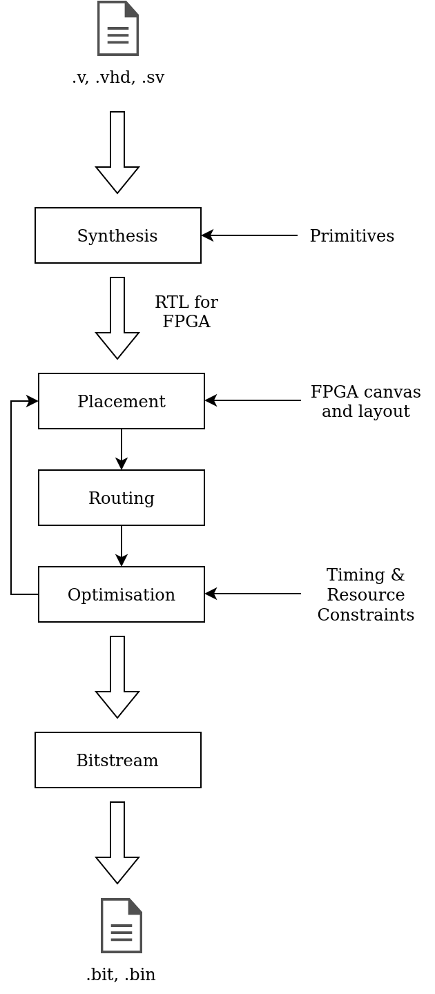
These tools transform the design until they have a binary to configure the FPGA: setting the LUT functions, connecting wires, and configuring the muxes.

The process begins by taking the HDL and performing transformations to use the primitives of the FPGA. This means all the logic and behaviours are mapped into the FPGA's logic cells, such as FFs, LUT, multipliers/DSPs, and block RAMs. Once the transformation is done. The transformed blocks (called pblocks) are placed into the FPGA layout. Then, the routing starts, connecting the pblocks to each other. Nevertheless, the placement and routing are iterative according to an optimiser that tries to meet the timing and area requirements by trying different placements and routing.
Once the placement and routing are finished, the bitstream is generated. With the bitstream, the final step is to configure the FPGA.
What's Next?
FPGA development also includes simulations. We are going to cover it in the following articles. Moreover, we will cover how to use C and C++ to implement hardware with the FPGA.
Stay tuned!
You may also want to visit our wiki: FPGA Minutes to Become an Expert
RidgeRun Is Here To Help You Reach The Next Level
RidgeRun has expertise in offloading processing algorithms using FPGAs, from Image Signal Processing to AI offloading. Our services include:
Algorithm Acceleration using FPGAs.
Image Signal Processing IP Cores.
Linux Device Drivers.
Low Power AI Acceleration using FPGAs.
Accelerated C++ Applications using AMD XRT.
And it includes much more. Contact us at https://www.ridgerun.com/contact.


